
Why OpenAI Built Its Own Silicon
Inference is where money leaves OpenAI. Every ChatGPT response, every Codex task, every API call burns compute — and until last week, all of that compute ran on Nvidia GPUs. For a company projecting $47 billion in annualized revenue and scaling toward gigawatt-scale data centers, that dependency is a structural problem. On June 24, 2026, OpenAI and Broadcom unveiled Jalapeño, OpenAI’s first Intelligence Processor — a custom ASIC designed from scratch to run LLM inference faster, cheaper, and at a scale that general-purpose GPUs weren’t built for.
The announcement is not just a hardware story. It’s a statement about what kind of company OpenAI intends to be. Greg Brockman, OpenAI’s President, framed it plainly: “By designing more of the stack ourselves, we can serve more intelligence with greater efficiency.” That’s the Google TPU playbook, the Apple Silicon playbook — control the substrate and you control the cost curve.
What Jalapeño Actually Is
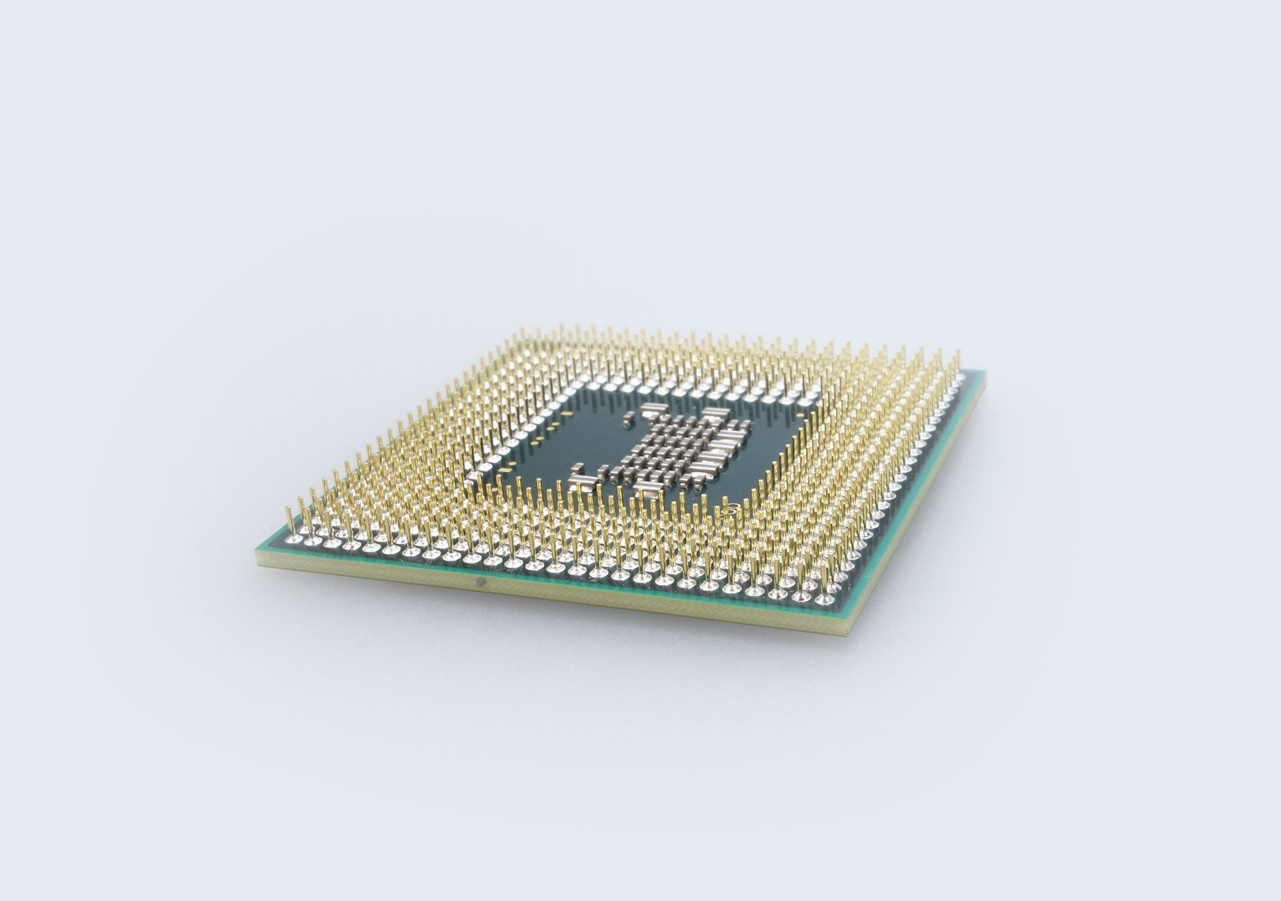
Jalapeño is a reticle-sized ASIC fabricated on TSMC’s 3nm process node. The die measures approximately 840mm², pressing right up against the ~858mm² limit of what an EUV scanner can print in a single exposure. It pairs a systolic-array compute structure — similar in concept to Google’s TPU line — with six to eight HBM3 or HBM4 memory modules. The architecture was designed specifically around the bottlenecks that matter for inference: data movement costs, memory bandwidth, networking efficiency, and the gap between theoretical peak performance and what hardware actually delivers in production.
Crucially, Jalapeño is not a repurposed training accelerator. Richard Ho, who leads OpenAI’s hardware program, was clear on this: the architecture is optimized around “the kernels, memory movement, networking, and serving patterns that matter most for frontier AI models.” OpenAI designed it around the systems it runs every day — ChatGPT, Codex, the API — and around its roadmap of future agentic products. Engineering samples were already running GPT-5.3-Codex-Spark workloads in the lab at production target frequency and power before the announcement.
The manufacturing partner is Broadcom for the silicon itself, with Celestica handling board, rack, and system integration. Broadcom’s Tomahawk networking silicon is part of the platform — a detail that matters at gigawatt scale, where interconnect latency becomes a real bottleneck.
Nine Months from Design to Tape-Out
The timeline is the most unusual part of this story. Jalapeño went from initial design to manufacturing tape-out in nine months — what OpenAI and Broadcom are calling the fastest ASIC development cycle ever achieved in high-performance advanced semiconductors. For context, custom AI chips typically take three to five years from concept to volume production. Google’s first TPU took years of internal development before going public. Nine months is not just fast; it’s a different category.
Part of the explanation is how OpenAI accelerated the design process itself. The company used its own AI models to speed up parts of the chip design and optimization work. This is the recursive AI story made concrete: the same models that will run on Jalapeño helped design Jalapeño. OpenAI has said this approach could have broader implications — if AI can help engineers design better chips faster, it lowers the cost of compute infrastructure across the industry, not just for OpenAI.
The other part of the explanation is deep software-hardware co-development. Because OpenAI’s engineering teams worked alongside Broadcom’s silicon experts from the start, the architecture reflects real workload data rather than generalized assumptions about what AI chips need. That tight loop between model teams, systems teams, and chip designers compressed what would normally be years of iteration.
The 50% Cost Claim and What It’s Worth
Early figures from OpenAI suggest Jalapeño will deliver roughly 50% lower inference cost per token compared to current Nvidia GPUs, along with substantially better performance per watt. Those numbers come with caveats: OpenAI explicitly noted it is still measuring final performance, and a detailed technical report will follow in the coming months. The 50% figure appears in reporting from TechTimes and other outlets, not in OpenAI’s own official announcement, which speaks more carefully of “substantially better” efficiency without a specific ratio.
Taking the claim at face value still requires context. Nvidia is not standing still. The Vera Rubin architecture and subsequent generations will close whatever gap Jalapeño opens. More importantly, a 50% inference cost reduction is only meaningful if OpenAI passes some of it to API customers — and that depends on business model decisions, not just engineering. The more realistic near-term outcome is that lower inference costs let OpenAI expand capacity, launch new products, or increase margins, rather than immediately halving what developers pay per million tokens.
What is clear is that the chip performs well enough in early testing to have justified the investment. Running production-frequency workloads in the lab before the public announcement is a meaningful threshold — it means this isn’t vaporware with a multi-year delivery horizon.
The Bigger Picture: Full-Stack AI
The strategic framing OpenAI is using — “building the full stack” — points to a specific competitive endgame. A company that controls its models, its software infrastructure, its hardware, and its products gains compounding advantages at each layer. It can co-design the chip around the model. It can co-design the model around the chip. Each optimization cycle compounds.
Jalapeño is the first step in a multi-generation compute platform. Initial deployment is targeted for the end of 2026, with full production ramp across 2027 and 2028. The infrastructure partner for that ramp is primarily Microsoft, which OpenAI is working with to build gigawatt-scale data centers — a scale that implies power and physical infrastructure commitments far beyond anything a single company has deployed for AI inference to date. Other unnamed infrastructure partners are also in the picture.
For agentic AI products specifically — the direction both OpenAI and Anthropic are moving — purpose-built inference hardware matters more than it did for chatbot-scale workloads. Running 1,000 parallel agents on a task demands not just raw throughput but low-latency, high-reliability inference with predictable cost. A chip designed around those patterns is better suited to the workload than a GPU designed primarily for throughput on large batch training jobs.
The most underrated detail in the announcement is Jalapeño’s stated flexibility: it’s designed to work with LLMs across the industry, not just OpenAI’s own models. That suggests OpenAI is thinking about offering inference-as-infrastructure to third parties — a business model extension that would put it in more direct competition with Google Cloud’s TPU offerings and AWS’s Trainium line. Nothing in the announcement confirms this direction, but the architecture decision is a prerequisite for it.
What Happens Next
The immediate unknowns are technical: the detailed performance report OpenAI promised will tell us whether the efficiency claims hold under real production load, across different model sizes and request patterns. The more important unknowns are strategic: how quickly Jalapeño reaches volume deployment, whether API pricing moves, and whether the multi-generation platform delivers the cost curve OpenAI needs to sustain its current growth rate while funding frontier model training.
What’s already clear is that the AI hardware market has a new entrant that is neither a chip vendor trying to build models nor a hyperscaler deploying commodity silicon. OpenAI’s vertical integration is now real, not just a roadmap slide. For Nvidia, the more interesting question than one chip’s benchmark numbers is what happens when the largest buyer of its inference hardware decides it doesn’t need to be a buyer anymore.
Further Reading
- OpenAI and Broadcom unveil LLM-optimized inference chip (OpenAI, June 24 2026) — the primary source, with quotes from Greg Brockman, Richard Ho, and Hock Tan.
- Tom’s Hardware: Jalapeño’s reticle-sized ASIC explained — the best technical breakdown of die size, process node, and architecture choices.
- CNBC: OpenAI and Broadcom reveal Jalapeño — market and competitive context, including Nvidia’s position and the Broadcom partnership terms.